Fine Ceramics
Hybrid Substrate for LED Carrier:
|
||||||||||||||||||||||||||||||||||||||||
|
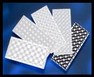
LED possesses characteristics of tiny size, high thermal shock resistance, high efficiency of luminosity and low power consumption, thus can be applied to visible light and invisible LED light (infrared rays). With respect to visible LED light, it applies to mobile phone, PDA, digital camera, traffic signal light, LCD backlight and green energy resources. Further, the neon lamp is expected to be replaced by newly-developed light bar. As for invisible LED light, it applies to remote controller of home appliances, high-quality stereo transmission, OA equipments, PC mouse, fire sensor, CO detector and infrared rays of express way tolling system etc.. HIC LED carrier developed by LEATEC processes high thermal dissipation and gas-tight characteristics, and thus could provide LED luminosity efficiency and long lifetime. Further its gas-tight characteristics enables harsh environment applications, especially for traffic light signal, outdoor display board, auxiliary illumination and main lighting etc., all of which can use HIC LED substrate to achieve best performance! |
||||||||||||||||||||||||||||||||||||||||
|
|
||||||||||||||||||||||||||||||||||||||||
Characteristic of HIC LED Carrie:
|
||||||||||||||||||||||||||||||||||||||||
|
||||||||||||||||||||||||||||||||||||||||
|
The presented value are typical material properties and were determined for test samples and follow testing standard. It may vary according to production configuration and manufacturing process. It do not a guarantee for certain properties. Leatec reserve the right to make technical changes.
|
||||||||||||||||||||||||||||||||||||||||
Design Rules for LED Carrier:
|
||||||||||||||||||||||||||||||||||||||||
|
||||||||||||||||||||||||||||||||||||||||


